1/13
August 2003
STP8NM60, STP8NM60FP
STD5NM60, STD5NM60-1
N-CHANNEL 600V - 0.9
- 8A TO-220/TO-220FP/DPAK/IPAK
MDmeshTM Power MOSFET
s
TYPICAL R
DS
(on) = 0.9
s
HIGH dv/dt AND AVALANCHE CAPABILITIES
s
100% AVALANCHE TESTED
s
LOW INPUT CAPACITANCE AND GATE
CHARGE
s
LOW GATE INPUT RESISTANCE
DESCRIPTION
The MDmeshTM is a new revolutionary MOSFET
technology that associates the Multiple Drain pro-
cess with the Company's PowerMESHTM horizontal
layout. The resulting product has an outstanding low
on-resistance, impressively high dv/dt and excellent
avalanche characteristics. The adoption of the
Company's proprietary strip technique yields overall
dynamic performance that is significantly better than
that of similar completition's products.
APPLICATIONS
The MDmeshTM family is very suitable for increase
the power density of high voltage converters allow-
ing system miniaturization and higher efficiencies.
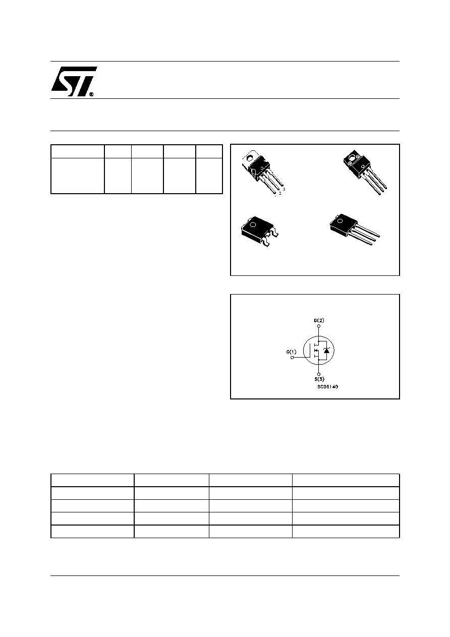
ORDERING INFORMATION
TYPE
V
DSS
R
DS(on)
I
D
Pw
STP8NM60
STP8NM60FP
STD5NM60
STD5NM60-1
600 V
600 V
600 V
600 V
< 1
< 1
< 1
< 1
8 A
8 A(*)
5 A
5 A
100 W
30 W
96 W
96 W
SALES TYPE
MARKING
PACKAGE
PACKAGING
STP8NM60
P8NM60
TO-220
TUBE
STP8NM60FP
P8NM60FP
TO-220FP
TUBE
STD5NM60T4
D5NM60
DPAK
TAPE & REEL
STD5NM60-1
D5NM60
IPAK
TUBE
TO-220
TO-220FP
1
2
3
1
3
DPAK
TO-252
3
2
1
IPAK
TO-251
INTERNAL SCHEMATIC DIAGRAM
STP8NM60, STP8NM60FP, STD5NM60, STD5NM60-1
2/13
ABSOLUTE MAXIMUM RATINGS
( ) Pulse width limited by safe operating area
(1) I
SD
5A, di/dt
400A/µs, V
DD
V
(BR)DSS
, T
j
T
JMAX.
(*) Limited only by maximum temperature allowed
THERMAL DATA
AVALANCHE CHARACTERISTICS
ELECTRICAL CHARACTERISTICS (T
CASE
=25∞C UNLESS OTHERWISE SPECIFIED)
ON/OFF
Symbol
Parameter
Value
Unit
STP8NM60
STP8NM60FP
STD5NM60
STD5NM60-1
V
DS
Drain-source Voltage (V
GS
= 0)
600
V
V
DGR
Drain-gate Voltage (R
GS
= 20 k
)
600
V
V
GS
Gate- source Voltage
± 30
V
I
D
Drain Current (continuous) at T
C
= 25∞C
8
8 (*)
5
A
I
D
Drain Current (continuous) at T
C
= 100∞C
5
5 (*)
3.1
A
I
DM
( )
Drain Current (pulsed)
32
32 (*)
20
A
P
TOT
Total Dissipation at T
C
= 25∞C
100
30
96
W
Derating Factor
0.8
0.24
0.4
W/∞C
dv/dt (1)
Peak Diode Recovery voltage slope
15
15
15
V/ns
V
ISO
Insulation Withstand Voltage (DC)
-
2500
-
V
T
j
T
stg
Operating Junction Temperature
Storage Temperature
-55 to 150
-55 to 150
∞C
∞C
TO-220
TO-220FP
DPAK
IPAK
Rthj-case
Thermal Resistance Junction-case Max
1.25
4.16
1.3
∞C/W
Rthj-amb
Thermal Resistance Junction-ambient Max
62.5
∞C/W
T
l
Maximum Lead Temperature For Soldering Purpose
300
∞C
Symbol
Parameter
Max Value
Unit
I
AR
Avalanche Current, Repetitive or Not-Repetitive
(pulse width limited by T
j
max)
2.5
A
E
AS
Single Pulse Avalanche Energy
(starting T
j
= 25 ∞C, I
D
= I
AR
, V
DD
= 50 V)
200
mJ
Symbol
Parameter
Test Conditions
Min.
Typ.
Max.
Unit
V
(BR)DSS
Drain-source
Breakdown Voltage
I
D
= 250 µA, V
GS
= 0
600
V
I
DSS
Zero Gate Voltage
Drain Current (V
GS
= 0)
V
DS
= Max Rating
V
DS
= Max Rating, T
C
= 125 ∞C
1
10
µA
µA
I
GSS
Gate-body Leakage
Current (V
DS
= 0)
V
GS
= ± 30V
±100
nA
V
GS(th)
Gate Threshold Voltage
V
DS
= V
GS
, I
D
= 250µA
3
4
5
V
R
DS(on)
Static Drain-source On
Resistance
V
GS
= 10V, I
D
= 2.5 A
0.9
1
3/13
STP8NM60, STP8NM60FP, STD5NM60, STD5NM60-1
ELECTRICAL CHARACTERISTICS (T
CASE
=25∞C UNLESS OTHERWISE SPECIFIED)
DYNAMIC
SWITCHING ON
SWITCHING OFF
SOURCE DRAIN DIODE
Note: 1. Pulsed: Pulse duration = 300 µs, duty cycle 1.5 %.
2. Pulse width limited by safe operating area.
Symbol
Parameter
Test Conditions
Min.
Typ.
Max.
Unit
g
fs
(1)
Forward Transconductance
V
DS
= I
D(on)
x R
DS(on)max,
I
D
= 2.5A
2.4
S
C
iss
C
oss
C
rss
Input Capacitance
Output Capacitance
Reverse Transfer
Capacitance
V
DS
= 25V, f = 1 MHz, V
GS
= 0
440
100
10
pF
pF
pF
C
oss eq.
(2)
Equivalent Output
Capacitance
V
GS
= 0V, V
DS
= 0V to 480V
50
pF
R
G
Gate Input Resistance
f=1 MHz Gate DC Bias = 0
Test Signal Level = 20mV
Open Drain
4
Symbol
Parameter
Test Conditions
Min.
Typ.
Max.
Unit
t
d(on)
t
r
Turn-on Delay Time
Rise Time
V
DD
= 300 V, I
D
= 2.5 A
R
G
= 4.7
V
GS
= 10 V
(Resistive Load see, Figure 3)
14
10
ns
ns
Q
g
Q
gs
Q
gd
Total Gate Charge
Gate-Source Charge
Gate-Drain Charge
V
DD
= 400V, I
D
= 5 A,
V
GS
= 10V
13
5
6
18
nC
nC
nC
Symbol
Parameter
Test Conditions
Min.
Typ.
Max.
Unit
t
d(off)
t
f
Turn-off Delay Time
Fall Time
V
DD
= 300 V, I
D
= 2.5 A
R
G
= 4.7
V
GS
= 10 V
(Resistive Load see, Figure 3)
23
10
ns
ns
t
r(Voff)
t
f
t
c
Off-voltage Rise Time
Fall Time
Cross-over Time
V
DD
= 480V, I
D
= 5 A,
R
G
= 4.7
,
V
GS
= 10V
(Inductive Load see, Figure 5)
7
10
17
ns
ns
ns
Symbol
Parameter
Test Conditions
Min.
Typ.
Max.
Unit
I
SD
I
SDM
(2)
Source-drain Current
Source-drain Current (pulsed)
8
32
A
A
V
SD
(1)
Forward On Voltage
I
SD
= 5 A, V
GS
= 0
1.5
V
t
rr
Q
rr
I
RRM
Reverse Recovery Time
Reverse Recovery Charge
Reverse Recovery Current
I
SD
= 5 A, di/dt = 100A/µs
V
DD
= 100 V, T
j
= 25∞C
(see test circuit, Figure 5)
300
1950
13
ns
µC
A
t
rr
Q
rr
I
RRM
Reverse Recovery Time
Reverse Recovery Charge
Reverse Recovery Current
I
SD
= 5 A, di/dt = 100A/µs
V
DD
= 100 V, T
j
= 150∞C
(see test circuit, Figure 5)
445
3005
13.5
ns
µC
A
STP8NM60, STP8NM60FP, STD5NM60, STD5NM60-1
4/13
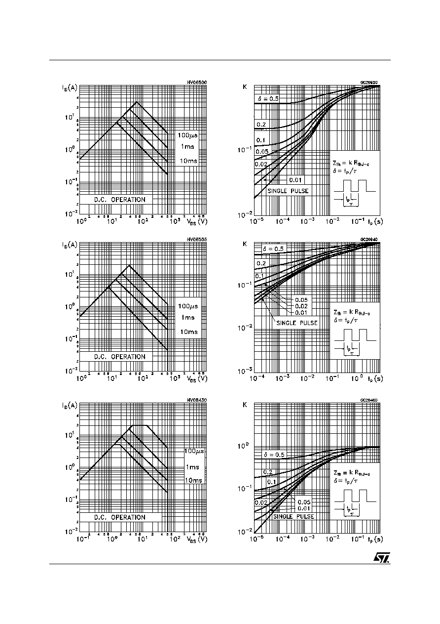
Safe Operating Area For TO-220FP
Safe Operating Area For TO-220
Thermal Impedance For TO-220
Safe Operating Area For DPAK/IPAK
Thermal Impedance For TO-220FP
Thermal Impedance For DPAK/IPAK
5/13
STP8NM60, STP8NM60FP, STD5NM60, STD5NM60-1
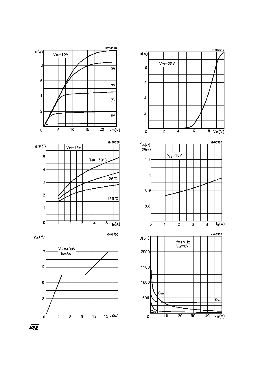
Transconductance
Static Drain-source On Resistance
Transfer Characteristics
Output Characteristics
Capacitance Variations
Gate Charge vs Gate-source Voltage
STP8NM60, STP8NM60FP, STD5NM60, STD5NM60-1
6/13
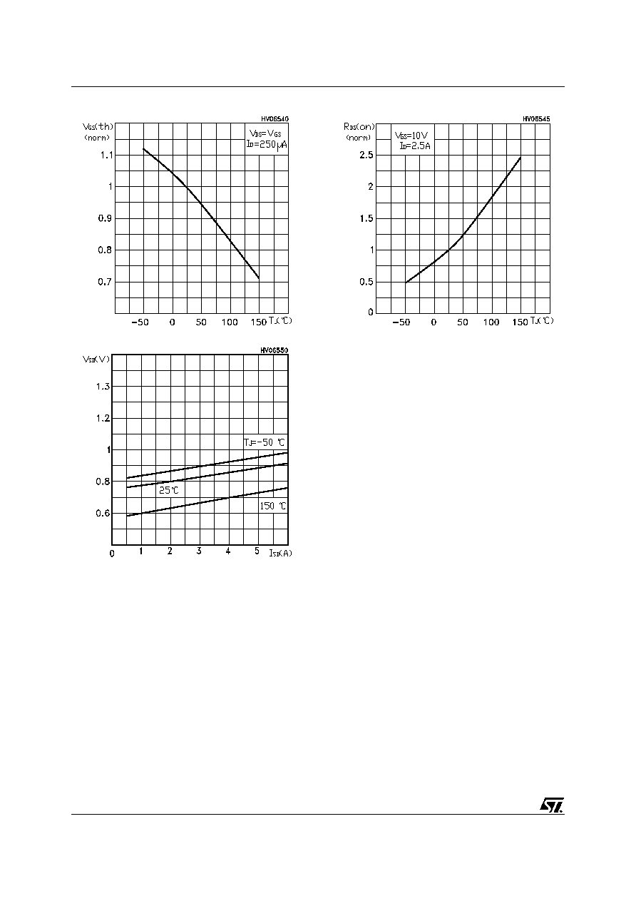
Normalized On Resistance vs Temperature
Normalized Gate Thereshold Voltage vs Temp.
Source-drain Diode Forward Characteristics
7/13
STP8NM60, STP8NM60FP, STD5NM60, STD5NM60-1
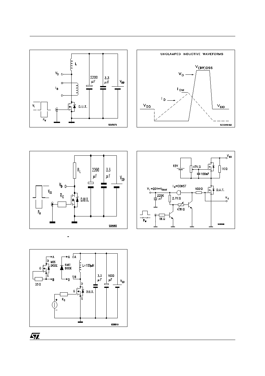
Fig. 5: Test Circuit For Inductive Load Switching
And Diode Recovery Times
Fig. 4: Gate Charge test Circuit
Fig. 2: Unclamped Inductive Waveform
Fig. 1: Unclamped Inductive Load Test Circuit
Fig. 3: Switching Times Test Circuit For
Resistive Load
STP8NM60, STP8NM60FP, STD5NM60, STD5NM60-1
8/13
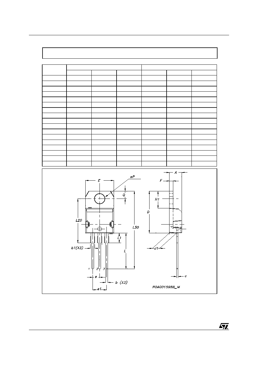
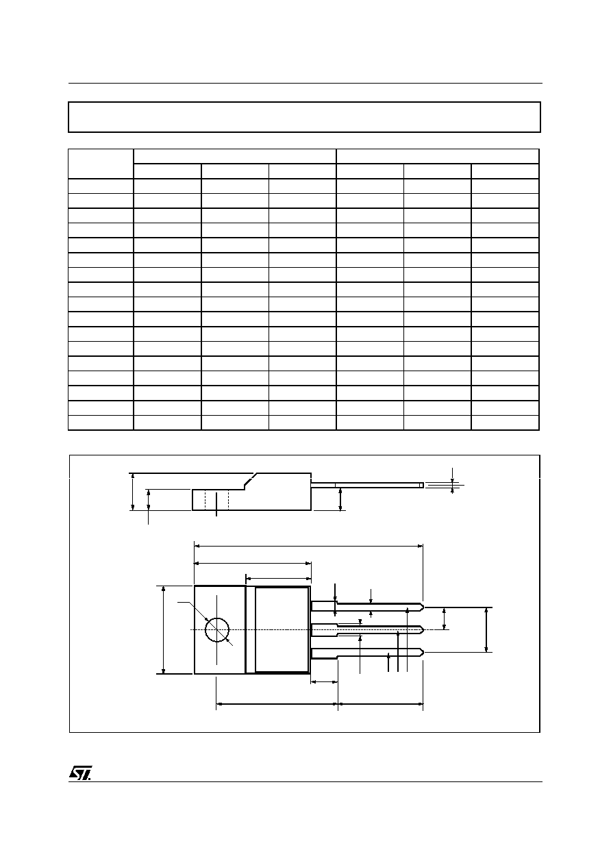
DIM.
mm.
inch
MIN.
TYP
MAX.
MIN.
TYP.
MAX.
A
4.40
4.60
0.173
0.181
b
0.61
0.88
0.024
0.034
b1
1.15
1.70
0.045
0.066
c
0.49
0.70
0.019
0.027
D
15.25
15.75
0.60
0.620
E
10
10.40
0.393
0.409
e
2.40
2.70
0.094
0.106
e1
4.95
5.15
0.194
0.202
F
1.23
1.32
0.048
0.052
H1
6.20
6.60
0.244
0.256
J1
2.40
2.72
0.094
0.107
L
13
14
0.511
0.551
L1
3.50
3.93
0.137
0.154
L20
16.40
0.645
L30
28.90
1.137
¯P
3.75
3.85
0.147
0.151
Q
2.65
2.95
0.104
0.116
TO-220 MECHANICAL DATA
9/13
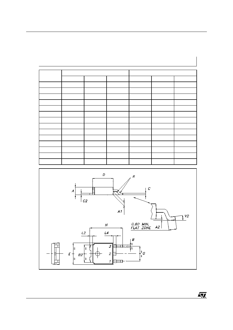
STP8NM60, STP8NM60FP, STD5NM60, STD5NM60-1
L2
A
B
D
E
H
G
L6
Ø
F
L3
G1
1 2 3
F2
F1
L7
L4
L5
DIM.
mm.
inch
MIN.
TYP
MAX.
MIN.
TYP.
MAX.
A
4.4
4.6
0.173
0.181
B
2.5
2.7
0.098
0.106
D
2.5
2.75
0.098
0.108
E
0.45
0.7
0.017
0.027
F
0.75
1
0.030
0.039
F1
1.15
1.7
0.045
0.067
F2
1.15
1.7
0.045
0.067
G
4.95
5.2
0.195
0.204
G1
2.4
2.7
0.094
0.106
H
10
10.4
0.393
0.409
L2
16
0.630
L3
28.6
30.6
1.126
1.204
L4
9.8
10.6
.0385
0.417
L5
2.9
3.6
0.114
0.141
L6
15.9
16.4
0.626
0.645
L7
9
9.3
0.354
0.366
ÿ
3
3.2
0.118
0.126
TO-220FP MECHANICAL DATA
STP8NM60, STP8NM60FP, STD5NM60, STD5NM60-1
10/13
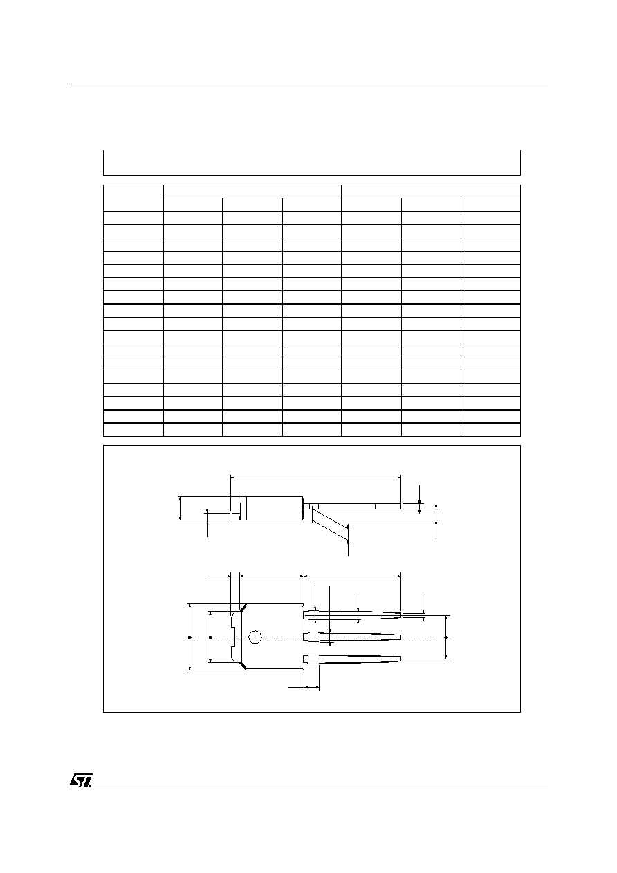
DIM.
mm
inch
MIN.
TYP.
MAX.
MIN.
TYP.
MAX.
A
2.20
2.40
0.087
0.094
A1
0.90
1.10
0.035
0.043
A2
0.03
0.23
0.001
0.009
B
0.64
0.90
0.025
0.035
B2
5.20
5.40
0.204
0.213
C
0.45
0.60
0.018
0.024
C2
0.48
0.60
0.019
0.024
D
6.00
6.20
0.236
0.244
E
6.40
6.60
0.252
0.260
G
4.40
4.60
0.173
0.181
H
9.35
10.10
0.368
0.398
L2
0.8
0.031
L4
0.60
1.00
0.024
0.039
V2
0
o
8
o
0
o
0
o
P032P_B
TO-252 (DPAK) MECHANICAL DATA
11/13
STP8NM60, STP8NM60FP, STD5NM60, STD5NM60-1
DIM.
mm
inch
MIN.
TYP.
MAX.
MIN.
TYP.
MAX.
A
2.2
2.4
0.086
0.094
A1
0.9
1.1
0.035
0.043
A3
0.7
1.3 0.027
0.051
B
0.64
0.9
0.025
0.031
B2
5.2
5.4
0.204
0.212
B3
0.85
0.033
B5
0.3
0.012
B6
0.95
0.037
C
0.45
0.6
0.017
0.023
C2
0.48
0.6
0.019
0.023
D
6
6.2
0.236
0.244
E
6.4
6.6
0.252
0.260
G
4.4
4.6
0.173
0.181
H
15.9
16.3
0.626
0.641
L
9
9.4
0.354
0.370
L1
0.8
1.2
0.031
0.047
L2
0.8
1
0.031
0.039
A
C2
C
A3
H
A1
D
L
L2
L1
1 3
= =
B3
B
B6
B2
E
G
= =
= =
B5
2
TO-251 (IPAK) MECHANICAL DATA
0068771-E
STP8NM60, STP8NM60FP, STD5NM60, STD5NM60-1
12/13
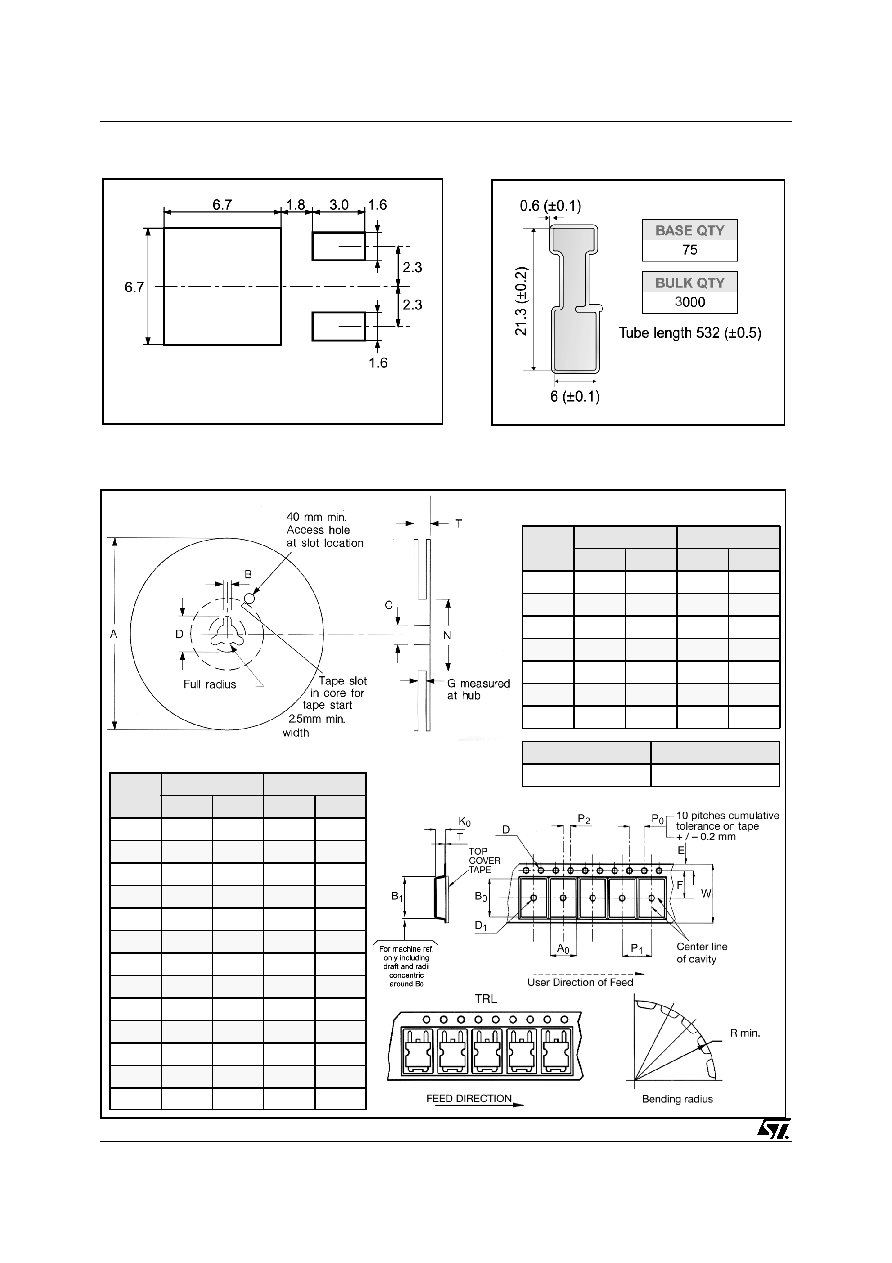
TAPE AND REEL SHIPMENT (suffix "T4")*
TUBE SHIPMENT (no suffix)*
DPAK FOOTPRINT
* on sales type
DIM.
mm
inch
MIN.
MAX.
MIN.
MAX.
A
330
12.992
B
1.5
0.059
C
12.8
13.2
0.504
0.520
D
20.2
0.795
G
16.4
18.4
0.645
0.724
N
50
1.968
T
22.4
0.881
BASE QTY
BULK QTY
2500
2500
REEL MECHANICAL DATA
DIM.
mm
inch
MIN.
MAX.
MIN.
MAX.
A0
6.8
7
0.267
0.275
B0
10.4
10.6
0.409
0.417
B1
12.1
0.476
D
1.5
1.6
0.059
0.063
D1
1.5
0.059
E
1.65
1.85
0.065
0.073
F
7.4
7.6
0.291
0.299
K0
2.55
2.75
0.100
0.108
P0
3.9
4.1
0.153
0.161
P1
7.9
8.1
0.311
0.319
P2
1.9
2.1
0.075
0.082
R
40
1.574
W
15.7
16.3
0.618
0.641
TAPE MECHANICAL DATA
All dimensions
are in millimeters
All dimensions are in millimeters

13/13
STP8NM60, STP8NM60FP, STD5NM60, STD5NM60-1
Information furnished is believed to be accurate and reliable. However, STMicroelectronics assumes no responsibility for the
consequences of use of such information nor for any infringement of patents or other rights of third parties which may result from
its use. No license is granted by implication or otherwise under any patent or patent rights of STMicroelectronics. Specifications
mentioned in this publication are subject to change without notice. This publication supersedes and replaces all information
previously supplied. STMicroelectronics products are not authorized for use as critical components in life support devices or
systems without express written approval of STMicroelectronics.
© The ST logo is a registered trademark of STMicroelectronics
© 2003 STMicroelectronics - Printed in Italy - All Rights Reserved
STMicroelectronics GROUP OF COMPANIES
Australia - Brazil - Canada - China - Finland - France - Germany - Hong Kong - India - Israel - Italy - Japan - Malaysia - Malta - Morocco
Singapore - Spain - Sweden - Switzerland - United Kingdom - United States.
© http://www.st.com